

hr369
Free Member
-
Joined
-
Last visited
Everything posted by hr369
-
 final price 30,101 with 50 bids. NOT bad if its legit.
 -
Famous for cheap cars. 10k is a rotten price for a 71
-
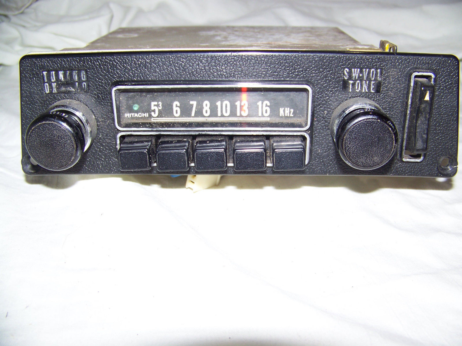
could you get away with a radio thats not as long? I just measured my factory hitachi radio and its 5" long. Perhaps it's shorter than that pioneer you've got now?
-
Why not reuse the old evap?
-
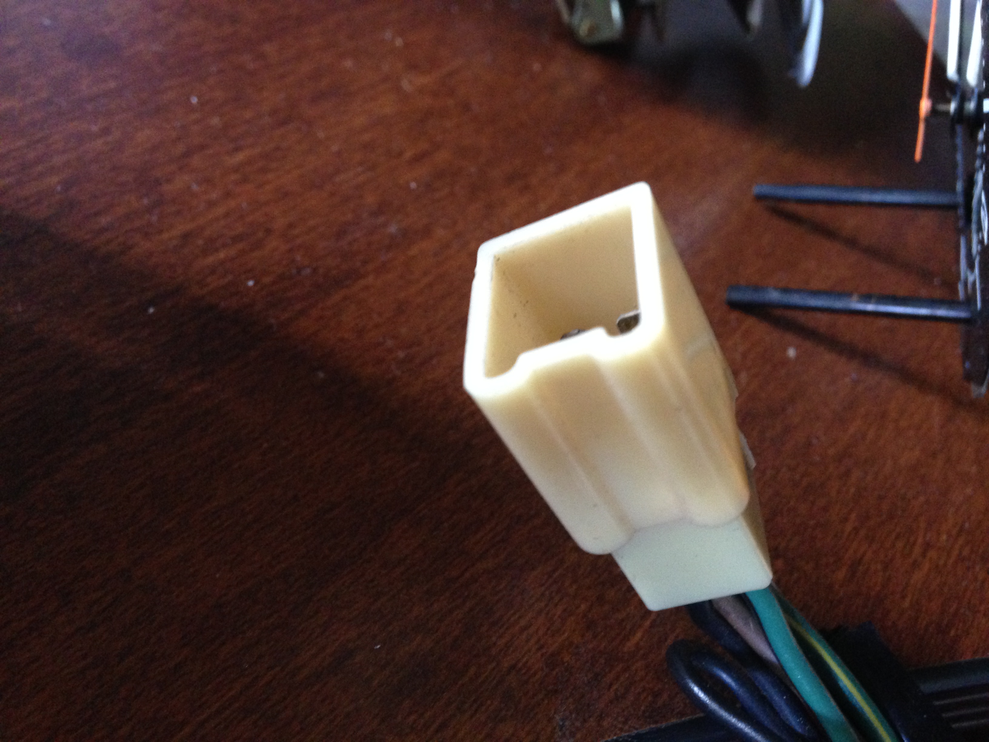
Then It would be option #2 for you. Yes, use an external box with the original style female connector. If you would like, Eric has volunteered to help people with soldering and pinouts.
-
He was a classy guy with a brilliant and wacky sense of humor. Watched a few of his last interviews on youtube just now. Sure wish they'de find a cure for alzheimer's
-
I gave 2 options for what he wants to do. 1). Keep the internal oscillator inside the clock 2). make a box for the purple oscillator. (external)
-
Thought he retired? Good to see he's still in business. I've bought good parts from him in the past too. Also good to see he brought one back that was "totalled"
-
Yea sorry cancel my order. I was going to try both but i'm very satisfied with the iteration of our version. How about gav240z's request to make the clock and harness interchangeable with the original oscillator? Can he do that with yours if the oscillator is inside the clock?
-
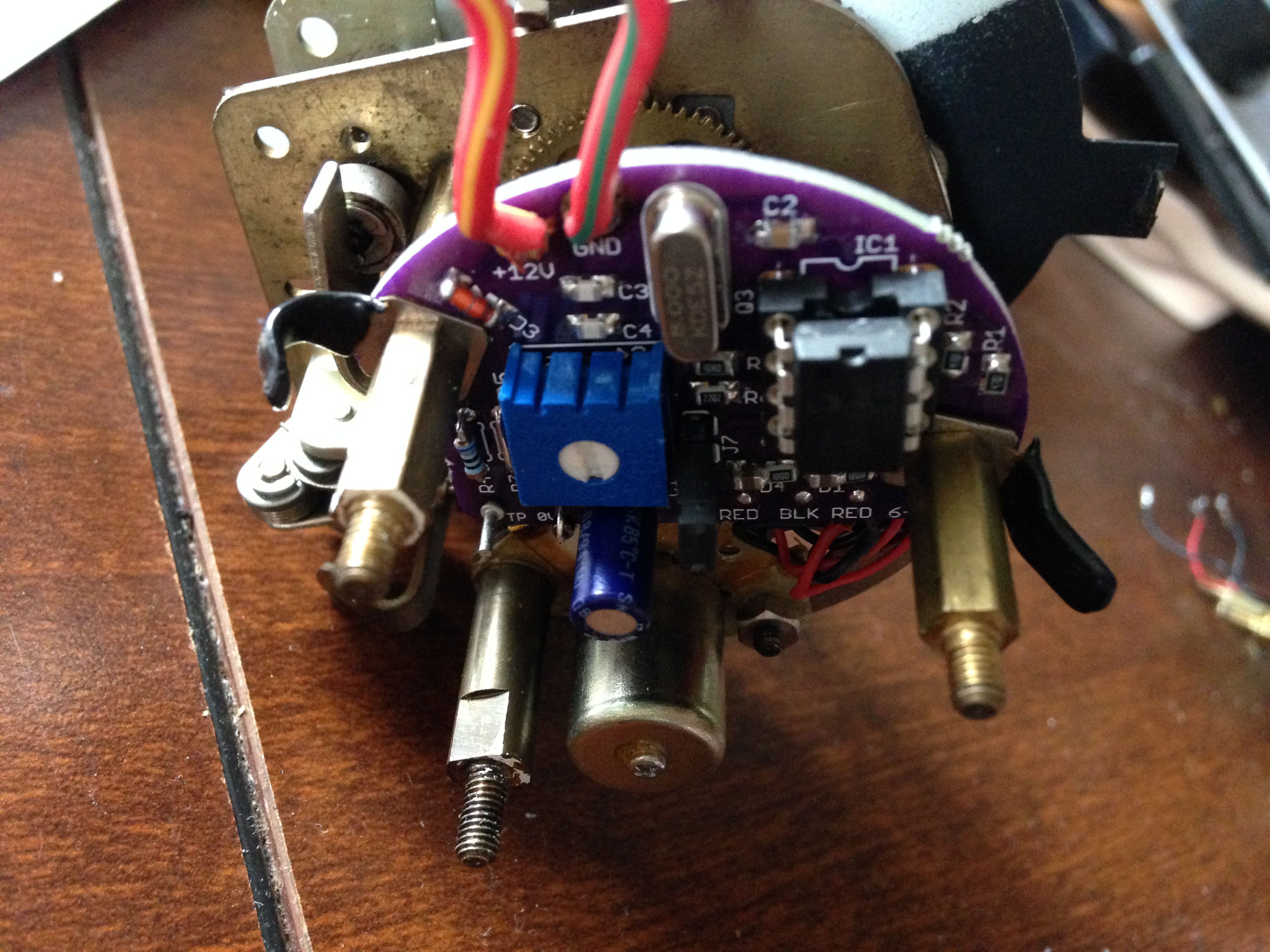
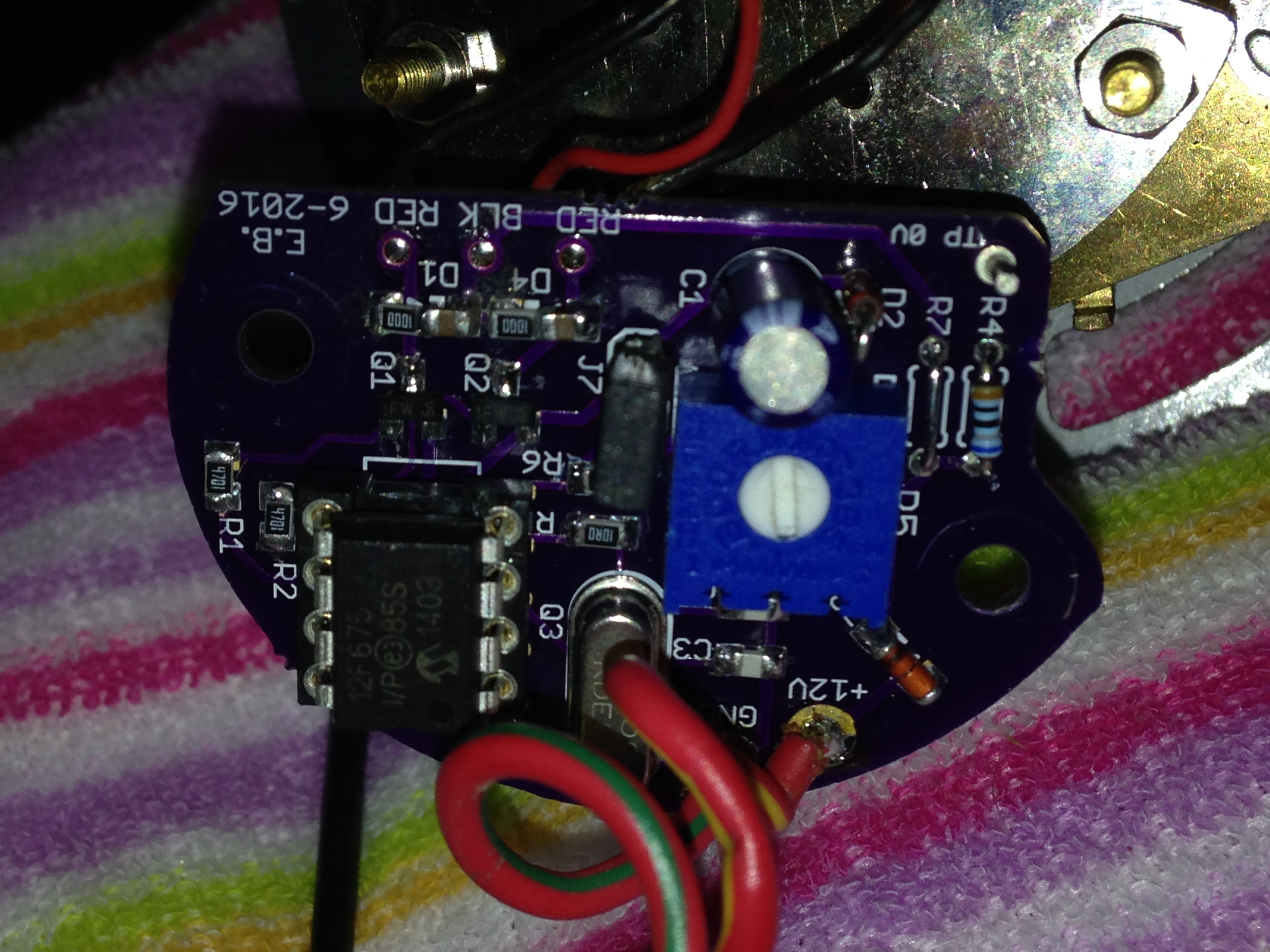
Take off the little pad where the harness and motor wires connect to. Solder 2 wires to the purple board power connectors. Solder 3 motor wires to the back side of the purple board. That's it for the soldering. I can now use a 240z tail light harness plug to plug into the original harness plug end that went into the original oscillator. Then pin your new female plug for + - and dash light. You could also just use your own harness. All you need is a power source and your dash light bulb. Then bench test it and make adjustments to the pot if necessary. you tell Eric he's going to die. He's younger than me! Your configuration would be difficult. First you would need to find a way to stack on the purple oscillator above the little soldering pads that i have removed on mine so that you could retain the original wiring. Then you would have to make a seperate power source + and - for the purple oscillator. The thing i'm not sure about is if you would have to isolate the 2 oscillators from each other even though the internal oscillator is powered down. I would have to ask Eric on that. Perhaps a switch to isolate them if needed. The easiest way of doing it your way would be to make a box for the purple oscillator.


-
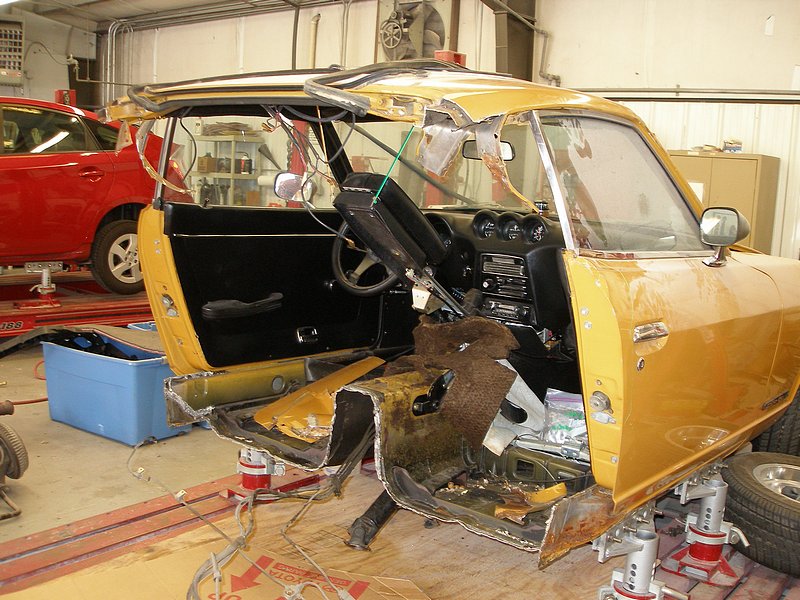
A few hours on the frame rack and that could be roughed out and ready for a new/used quarter. Even at home i've pulled out some pretty kinked up quarters with my homemade I-beam and 20 ton ram. I have seen people go to extremes to not show any collision damage but if he's willing to put up with a few bumps and waves in the floor then by all means its fixable with just a quarter panel and tail lite panel replacement.
-
That car looks very fixable.
-
good to know hitachi's can be fixed by touching up cold solder joints. Wave soldering defect perhaps.
-
The label is just a warning to mount the tires from the back side to prevent scratching this might have a little info. link to kyushashoes.com
-
The good new is you can buy a $30 jammer to plug into a cigarette lighter when you rent a car and sometimes go off-roading or very fast. They won't know a thing.
-
bad news. they can just tape a rf signal jammer to the side of your car and drive off into the night. crap.
-
But the device is easier to get at inside a boat right? whereas in a car they have to get inside without setting off the car alarm and then there are lots of places behind door panels, interior panels to hide the device. There are lots of video's on youtube where people have tracked their stolen cars and have brought police to that location to recover it. Our old datsun's hopefully will never attract this caliber of thief.
-
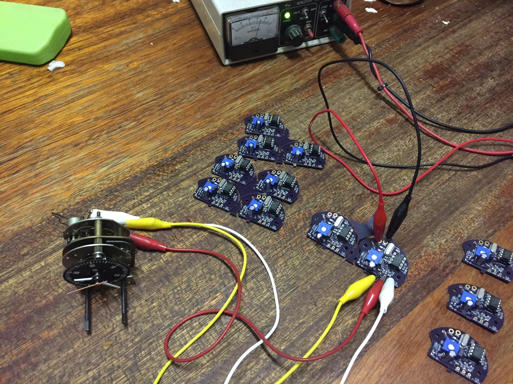
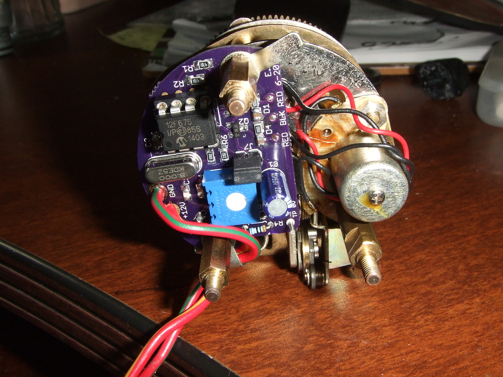
Update: I've had to tweak the pot just a tad to run my clocks accurately. However this is bench testing with an almost constant temperature of 80F.So far i've tested it on 3 clocks and i'm satisfied with the oscillator. I don't know why it needed the little tweak. Eric sent it to me with the slot at 12 o clock. As you can see its at about 11:59. But more importantly,all clocks run good on this setting. No need for me to tweak for each individual clock. Other people will need to bench test their and adjust accordingly if needed. He has graciously assembled the boards that you see below and will be sending them in a few days. Eric suggested a price of 98.50 usd + shipping. Sounds fair? any takers?


-
i've found that many bad reviews can be by customers that expect precision quality in a cheap china crap 20$ electronic or simply don't know how to use the thing. Some didn't realize that the battery didn't last a month before needing a recharge/new battery. Just to test the technology i was considering the cheaper one. There are a few remote areas around me that have no cell service. With my luck, thats where all the car thieves live
-
I was thinking about getting one of these. You only pay for gsm cellular data service month to month. Verizon has a plan thats real cheap i believe. amazon auction or a more sophisticated system that allows remote control functions. It says you can turn on the alarm remotely so i would imagine you see real time where the car is at and if it's traveling you could kill the ignition and they would have to abandon the vehicle in the road. A more suitable function would be to send a 1000volt shock to their arse. amazon auction
-
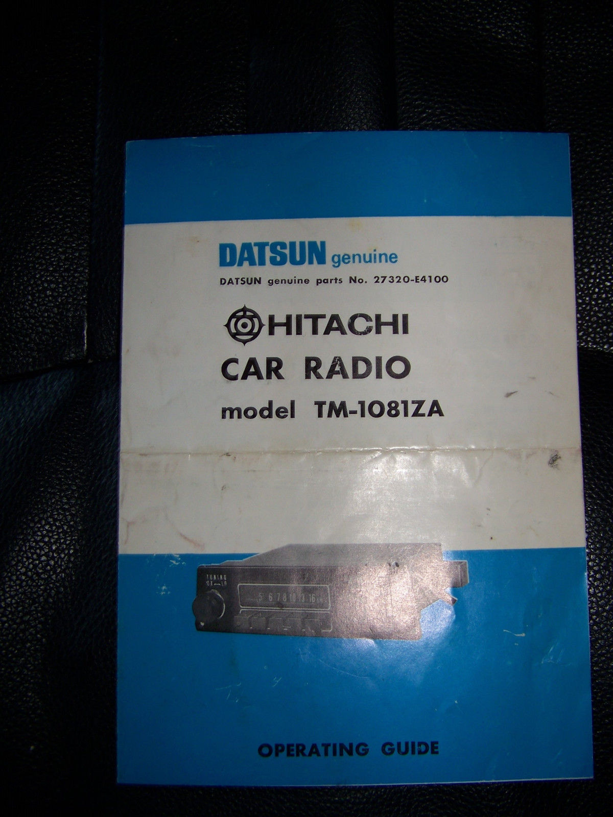
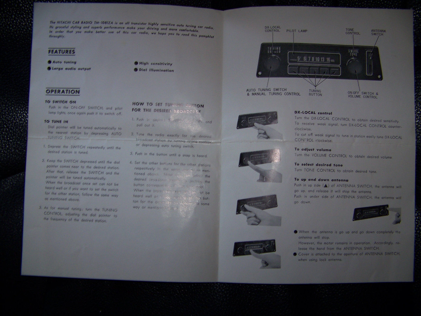
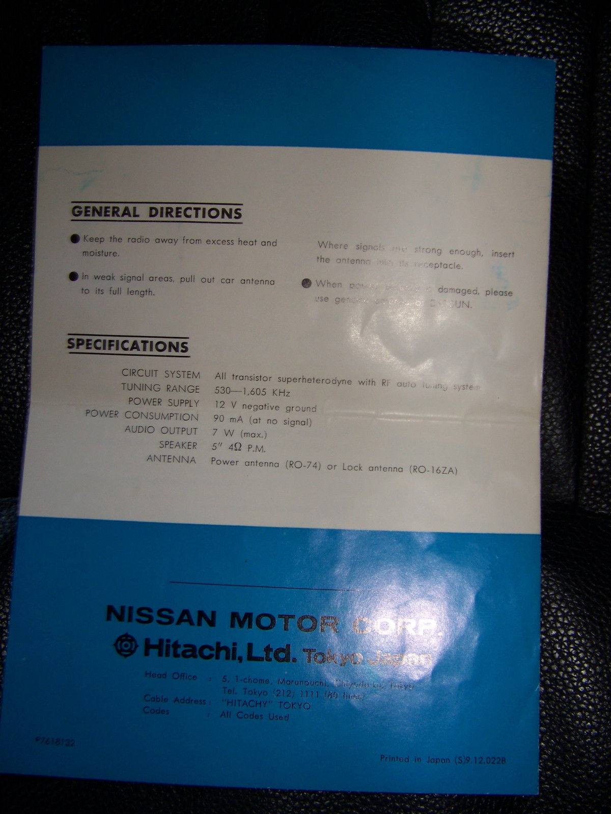
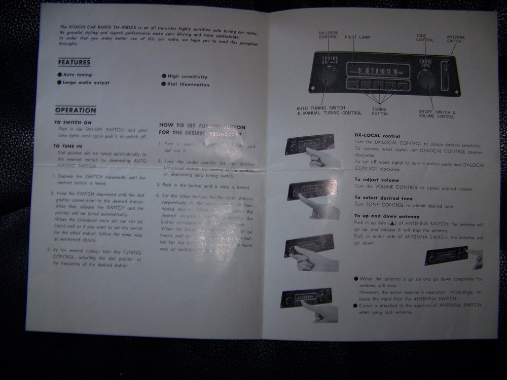
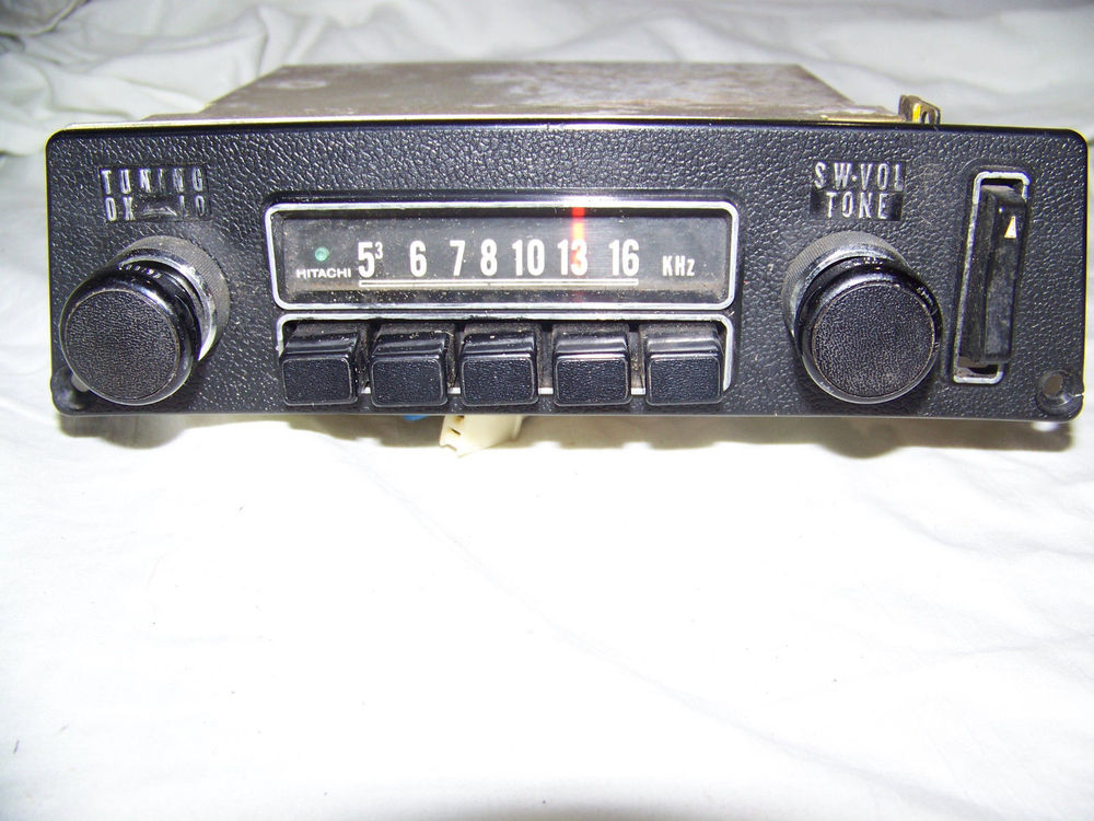
Ran across this manual the other day. Strange, you guys must have gotten the older radio's. They just put a later model label on them perhaps. Your ZB's have a green light and our ZA's have a green light. Original OEM Series One (1969-70) Datsun 240Z Hitatchi AM Signal Seeking Radio from my own early 1970 240Z. This factory radio was removed a few months after delivery in the summer of 1970 and placed in safe storage since. I had kept it all these years in case I decided to put it back in the 240Z, which after 46 years now I realize I never will. The radio is intact, faceplate, knobs and buttons are in excellent condition, even the original antenna switch is present! Even the original spare fuse is still in it's plastic envelope! It has not been fully bench tested but does power up. AS A BONUS, I will include the original Hitachi instruction booklet that was sold with the car. Try to find one of these today!


-
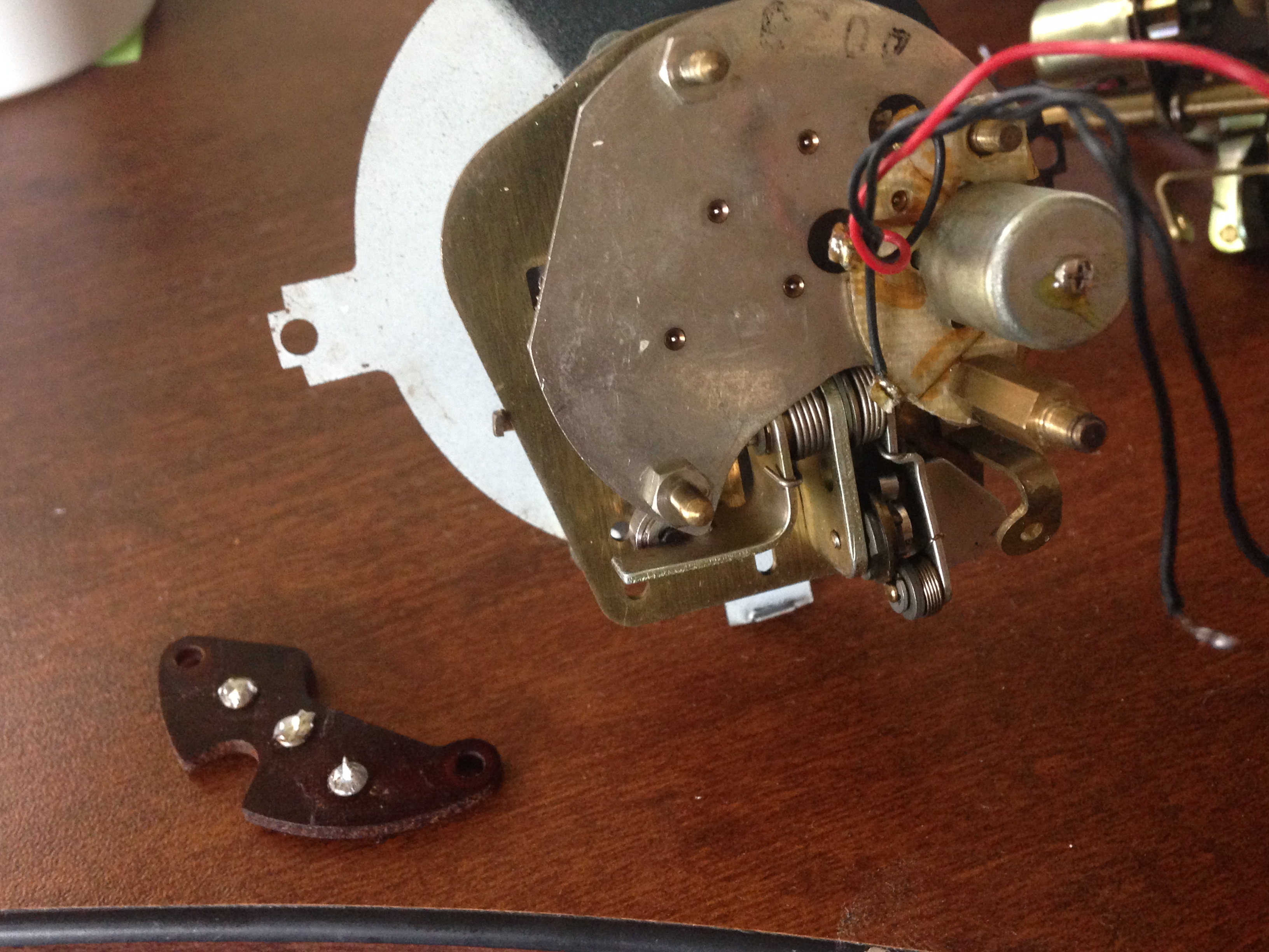
Update time. I've received the purple pcb oscillator and installed it. It's way smaller that it looks in the pictures. It took about 20 minutes to solder in the new board and bolt it in. I will be testing it with my other clocks to see how accurate it is. Right now i've had it running a couple hours and its keeping accurate time. It has built into it, reverse polarity protection for those of us that are electronically challenged, myself included. I've ordered a small amount of boards as I don't anticipate many people will need them. clock running with new purple oscillator Reverse engineering this clock and running it on 21'st century electronics was no small feat. Here is some of the C code that Eric wrote for the prototype and resides in the little IC chip. AWESOME work he does. __________________________________________________________________________________________________________________________________________________ #include <htc.h> #include <xc.h> //#include <float.h> // do I need this? #define _XTAL_FREQ 4000000 // Internal Oscillator... for now. Required // for __delay_ms function /* The configuration bits can be set in the IDE 'Configuration Bits' window, * or they can be set here. */ // PIC12F675 Configuration Bit Settings: /* CONFIG */ #pragma config FOSC = INTRCIO // Internal oscillator. #pragma config WDTE = OFF // Watchdog Timer disabled. #pragma config PWRTE = OFF // Power Up timer off. #pragma config MCLRE = OFF // MCLR pin disabled, I/O function of GP3. #pragma config BOREN = OFF // Brown-out detect off. #pragma config CP = OFF // Program memory code protection off. #pragma config CPD = OFF // Data memory code protection off. unsigned int pulse_width_count = 0; // Used to adjust pulse width. volatile unsigned int T_pot_setting; // Most sig 8-bits from pot ADC conversions. volatile unsigned int F_pot_setting; // Use all ten bits, so need 16-bit word. volatile char outputs; // bit0 for output 0 (GP0), bit1 for output 1 (GP1). volatile unsigned int analog_reading; // The 10-bit ADC result. /********************************* SETTING UP ************************************/ /*********************************************************************************/ void init_ports(void){ // Set input & output pins: GP2 (AN2) and GP4 (AN3) set as inputs for analog signal, // GP3 can only be input. TRISIO = 0b00011100; // Comparators off. CMCONbits.CM = 0b111; // Analog input register ANSEL set in setup_ADC() below. } //////////////////// void setup_osc(void){ ; // Nothing to do here. The oscillator is set above by setting the FOSC bits. // OSCCAL = 0x00; // Shouldn't be needed. } //////////////////////// void setup_timer1(void){ // Timer1 is 16-bit. It will count to 65535 before overflowing. // With a 4MHz internal clock (Fosc), the instruction clock operates at 1MHz: // (Fosc/4, so Tcyc = 1usec). // With a desired interrupt time of 11.43msec, we have 11430 instruction cycles, // which is under the 65535 cycles possible with Timer1. So using Timer1 should be // fine! T1CONbits.TMR1ON = 1; // bit 0 = 1: TMR1ON -> turn timer on. // bit 1 = 0: TMR1CS -> Clock source = Fosc/4. // bit 5,6 = 00: T1CKPS -> prescaler = 1:1 - no scaling. } ///////////////////// void setup_ADC(void){ // Pulse_Width is analog input on AN2. // Pulse_Frequency is analog input on AN3. // Set ADCON0 configuration bits: // ADFM = 1 : ADC result right justified as we will use all ten bits. Two most // sig bits in ADRESH, the eight least sig bits in ADRESL. // VCFG = 0 : ADC reference is Vdd pin.. for now. // <CHS1:CHS0> = 0b10 (2dec) to select AN2 input, (<CHS1:CHS0> = 0b11 3dec) for // AN3 input. // ADON = 1 : Turn on the ADC. ADCON0bits.ADFM = 1; // ADC result right-justified. ADCON0bits.CHS = 3; // Select AN3 for ADC for first conversion (freq). ADCON0bits.ADON = 1; // Turn on the ADC. // Set ANSEL configuration bits: // <ADCS2:ADCS0> = 101 for 4us TAD conversion time (datasheet recommended for 4MHz // clock). Analog input on AN2 (GP2) set for pulse time adjustment pot, and AN3 // (GP4) for frequency adjustment pot. ANSELbits.ADCS = 0b101; } /**************************** INTERRUPT SERVICE ROUTINE ***************************/ void setup_timer1_interrupt(void){ // Timer1 is a peripheral, so peripheral interrupts must be enabled // (and also global interrupts). TMR1IF = 0; // Clear Timer1 Interrupt Flag. PIE1 = 1; // Enable Timer1 Interrupt. PEIE = 1; // Enable Peripheral Interrupts. GIE = 1; // Enable Global Interrupts. } void interrupt ISR(void){ // Interrupt Service Routine // This interrupt it called at twice the motor (electrical) frequency. // Timer1 has timed out so we must aternate the GP0 and GP1 outputs. // The interrupt activates on overflow, so the starting value of the timer // must be determined to get the correct timer period. Calculations at end // of code. // Here we read and manipulate the last ADC result and initiate the next ADC // conversion. We will perform ADC on the two analog inputs alternately // (one for pulse frequency, and one to control the pulse width) // In reversing the pin polarity, the pins themselves are not reversed as they // might both be 0 (as the expiration of pulse_width_count will set both outputs // to zero). So 'outputs' records the last setting of output pins, and it is // 'outputs' that is reversed. This is then copied to the GPIO pin register. TMR1 = (0xDC00 - F_pot_setting); // Reset TMR1. outputs = outputs^0b00000011 ; // XOR - reverse outputs for GP0 and GP1. GPIO = outputs; // Assign 'outputs' to actual output pins. // Alternately update the Frequency setting (F_pot_setting) and pulse width // (T_pot_setting). if ((outputs & 0x01) != 0){ // Set pulse width. analog_reading = ADRESL + (ADRESH * 256); // Change 10-bit value to 8-bit T_pot_setting = (analog_reading >> 2); // value (max 255). ADCON0bits.CHS = 3; // Change A/D channel to measure Frequency pot // next time around. __delay_us(50); // Delay after channel swap, avoids cross-talk. } else{ // Set pulse frequency. analog_reading = ADRESL + (ADRESH *256); F_pot_setting = (analog_reading << 1); // Mult by 2 to scale to 0x7FE. ADCON0bits.CHS = 2; // Change A/D channel to measure pulse width pot // next time around. __delay_us(50); // Delay after channel swap, avoids cross-talk. } ADCON0bits.GO_DONE = 1; // Start next A/D conversion. pulse_width_count = 0; // Reset counter for pulse width. // GPIO5 = 1; // Turn on LED at GP5 - program running. TMR1IF = 0; // Reset Timer1 overflow interrupt flag. return; } /********************************** MAIN PROGRAM **********************************/ /**********************************************************************************/ void main() { setup_osc(); init_ports(); setup_timer1(); setup_timer1_interrupt(); setup_ADC(); outputs = 0b00000001; // Initialise output pulses variable with pulse // at GP0. GPIO = outputs; // Write to GPIO register. // Turn on LED at output GP5 - program running. while(1){ pulse_width_count++; // Delay chosen so that that 255 (0xFF) __delay_us(28); // increments take up the full 11.4 millsec. if (pulse_width_count > T_pot_setting){ GPIO = GPIO & 0b11111100; // Turn off outputs. GPIO5 = 1; // debug - turn on LED pulse_width_count = 0; // Reset so we don't keep coming back. } // if } // while } // main /* Determining the Timer1 starting value for interrupt for clock frequency: * * The clock I tested needs the outputs to be alternated every 11.43 millisec * for the clock to operate at about the right speed. * The microcontrller clock speed (Fosc) is set to 4MHz in the config parameters * at the start of the program. Timer1 increments with each instruction cycle which * is equal to Fosc/4 = 1MHz, so it increments at 1 microsec intervals. For 11.43 * millisec, the clock increments 11430 times. As the timer interrupts at overflow, * then the timer must start at 65535 (0xFFFF) minus the 11430. * 65535 - 11430 = 54105 (0xD359) approx. * The result from the A/D converter is 10-bit, i.e. 0-1023 (0x00 - 0x3FF). * This permits an adjustment time of about 1 millisec. If I want an adjustment * time of +/- 1 millisec (2 millisec) then I will double the A/D conversion result. * So the timer starting point will have to be about 0xD539 + 0x3FF, so that up * to 2 * 0x3FF can be subtracted from it. So starting point will be about 0xD938. * This is approximate as there will be some latencies in processing the code, etc * The final value will be higher and determined experimentally. So we should * have a range of about 9.4 millisec to 11.4 millisec with the 'correct' * 10.4 millisec setting when the control pot is set to the middle position. * * Determining pulse width: * * The output of the pulse width pot is saved as an 8-bit value: 0xFF (255 decimal). * At lowest frequency, the pulse width above will be up to 11.4 millisec, so we * need the pulse width counter to increment at 45 microsec at a time (45us * 255 * = 11.5 ms. An added delay of 28 microsec resulted in desired increment delays . * */
-
I haven't noticed that. All fairlady or just 432? There is one 432 that just keeps expiring and relisting. This is a new one to me. He's willing to export., Overseas people will pay more. Is Edward Lee still in business? He had some red hot deals red hot deals yahoo link

-
He sent back the radio and made this video. He said it worked good right out of the box. I'm not sure what's going on. It could have been the new RF transistor fixed it and when i retested it, my battery voltage was too low. I don't know for sure. It looks like he cleaned a bit inside the antenna jack but that shouldn't make this much of a difference. I'm now getting radio stations acouple hundred miles away in honolulu. https://www.youtube.com/watch?v=_KGtGCfOufE&feature=youtu.be Some of the 200sx here had radio's with the RN designation.
-
When I lived in calif there were people that had family living in rural areas of calif and they registered their modified cars in those non smog counties. Pain in the butt tho. I'de rather have stock exhaust.